
In this post I provide a brief introduction to NAND Flash memories, a technology that has come to dominate the semiconductor memory market since its inception in the 1980s.
1. Intro to NAND Flash
The two major architectures of Flash memory are NAND memories and NOR memories. These names allude to the fact that their memory arrays are organized somewhat like NAND and NOR CMOS logic gates. The first modern Flash memory was introduced by Masuoka and his collaborators at Toshiba in the 1984 IEEE International Electron Devices Meeting. Initially, Flash memory chips were envisaged as a potential replacement for the EPROM (“Erasable Programmable Read Only Memory”) chips that dominated the market at the time. Most EPROMs then available required exposure to ultraviolet light to have their data erased; Flash memories, on the other hand, could be erased electrically. The very name “Flash” was chosen because these memories could have their content deleted much more quickly than other technologies available at the time (Bez et al., 2003). Mass production of NAND Flash memory began in 1992, with the introduction of a 16 megabit chip produced with 0.7-
Applications of Flash memory expanded at a rapid pace due to the various advantages of this technology: nonvolatility, fast access, and robustness. Flash memory applications can be divided into two major niches. The first is for code storage applications such as personal computer BIOS and cellular phones; NOR-type cells are better suited for these applications in view of their superior random access speed. The second is for file-storage applications such as the digital still camera, the smartphone, and the tablet PC; NAND-type cells have become the storage technology of choice for this market segment. Indeed, some of the most groundbreaking consumer electronics innovations of the previous 20 – 30 years would’ve been a lot harder to achieve, if not impossible, without extensive reliance on NAND Flash memory technology. This applies to the transition from floppy disks to the USB drives employed in portable data storage; to the transition from cellular phones to smartphones; and to the miniaturization of personal computers to tablet computers. Figure 1 drives this point home.
Figure 1. NAND Flash and new technologies

Up until the mid-2000s, NAND Flash technology was behind NOR Flash in terms of market share, but has since supplanted it. Nowadays NOR tech is mostly restricted to applications that involve storage of computer data destined to be executed directly (“execute in place” or XiP-type operation). Intel, ST Micro, and Spansion (now Cypress Semiconductor) are some of the main suppliers of NOR Flash products, while Toshiba and Samsung are the major suppliers of NAND Flash devices.
While other semiconductor memories have been on a cadence for new process technology development usually greater than 2 years (i.e., slower than predicted by Moore’s Law), NAND Flash memories have evolved at a substantially faster pace. Indeed, in the early 2000s Hwang Chang-gyu of Samsung outlined an aggressive roadmap for his company, establishing that the bit density of NAND Flash memories had to double every year. Some in the Flash community have come to refer to this postulate as “Hwang’s Law” (Dieter, 2014), a clear reference to Moore’s Law, the famous model that predicted the exponential evolution of electronic device complexity in recent decades. Indeed, Dimitrakis (2015) states that in recent years NAND Flash was the only semiconductor memory technology still evolving at a pace comparable to Moore’s Law.
2. Organization of NAND Flash memory
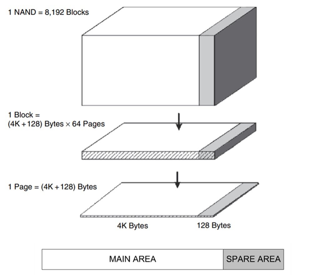
The internal organization of a NAND Flash memory chip is not that much different from that of other memory circuits. As illustrated in Figure 2, a memory is divided into pages and blocks. A block is the smallest erasable unit. Each block contains multiple pages. The number of pages within a block is typically a multiple of 16 (e.g., 64, 128). A page is the smallest addressable unit for reading and writing. Each page is composed of main area and spare area; the main area can range from 4 to 8 kilobytes, or even 16 kB. The spare area can be used for error-correcting codes (see below) and is of the order of a couple of hundreds of bytes for every 4 kB of main area.
Every time an operation is to be executed on a NAND device, we must issue the address in which we want to act. As with typical memories, the address is divided in a row and a column component. Row address identifies the addressed page, while column address is used to identify the bytes inside the page.
Figure 2. Organization of NAND Flash memory.
The NOR memory array is addressed by random access, which means that each cell can be addressed individually, whereas for NAND memories this is done sequentially. As a result, erase speeds tend to be higher for NAND Flash than for NOR Flash. In contrast, reading is faster for NOR tech than for NAND devices. In applications that read data sequentially, such as audio/video playback or data logging, sequential operation is an asset and NAND Flash becomes an attractive technology. However, if random accesses are required, as in the case of code execution, NAND memories do not perform nearly as well.
3. Floating gate technology
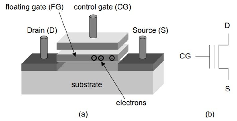
The most popular Flash memory cell is based on the floating gate (FG) technology, which is illustrated in Figure 3. In such a device, a MOS transistor is built with two overlapping gates rather than a single one; the first one is completely surrounded by oxide, while the second one is contacted to form the gate terminal. The isolated gate constitutes an excellent “trap” for electrons, which guarantees charge retention for years. The operations conducted to inject and remove electrons from the isolated gate are called program and erase, respectively. Applying a fixed voltage to the cell’s terminals, it is then possible to distinguish between two storage levels: when the gate voltage is higher than the cell’s threshold voltage Vth, the cell is on; otherwise, it is off. Programming of NAND cells is based on Fowler-Nordheim (FN) tunneling, a quantum-mechanical mechanism of electron tunneling under strong electrical fields. The small oxide layer between the transistor channel and the floating gate is appropriately called “tunnel oxide” because electron transport occurs through it. FN tunneling of cold electrons will occur when a field on the order of 8 to 10 MV/cm is established across the insulator next to the floating gate (Brewer and Gill, 2008). Depending on the polarity of the electric field, electrons can be directed into or out of the floating gate, leading to storage or erasure of data.
Figure 3. Floating gate MOSFET.
Another common mechanism of charge transfer in memory cells is channel hot-electron (CHE) injection, which can be employed to add electrons to a floating gate (i.e., programming). CHE injection is faster than FN tunneling, but it is more difficult to control and less efficient. CHE is employed primarily in NOR devices and finds no application in modern NAND Flash memories.
In spite of its apparent simplicity, manipulation of floating gates in memory cells can be complicated by several factors. The erase operation presents some issues of particular concern. First, erasing shifts the threshold voltage negatively from a positive value to a value nearer to zero; if continued too far, the threshold voltage can go through zero and become negative. This phenomenon, known as overerase, causes the transistor to change from enhancement mode to depletion mode. Second, the erase process is sensitive to the initial state of the transistor. Erase voltages are applied to transistors located in the same tub simultaneously. If some of those transistors are in a programmed state while others are in the erased state, the resulting final threshold voltages will have quite a spread. It is likely that for some operations overerase will occur. To manage this situation, it is common practice to program all transistors before applying an erase voltage.
As with every digital memory technology, reliability is an essential requirement of floating-gate Flash memories. The general criterion is that the programmed threshold voltage Vth does not decrease 10% over a product-relevant time of 10 years. The number of stored floating gate electrons in a 50 nm FG NAND device for a threshold voltage shift of Vth = 4 V is about 600. Accordingly, a 10% loss criterion over a period of 10 years results in a tolerable loss of one electron every two months, or a leakage current of 3
In principle, there are multiple leakage paths that could lead to a loss of the programmed floating-gate electron charges, but the most vulnerable route is usually the leakage of electrons through the tunnel oxide, which, after all, is intended to be the only pathway for electron transport in the memory cell during programming or erasing. What’s more, the TOX is the thinnest dielectric layer in the floating gate configuration. Successive programming and erasing cycles leads to the formation of so-called oxide traps in the TOX; these are broken bonds of the atoms in the oxide matrix that occur as byproducts of electron tunneling processes. The density of traps increases with successive program/erase cycles, a condition known as oxide stress.
Other sources of electron loss in floating-gate devices exist, and, in contrast to tunnel oxide leakage, have been reduced to acceptable levels as technology progressed. For one, electrons can be trapped in the insulating layers surrounding the floating gate during wafer processing as a result of so-called plasma damage, or even during the UV exposure normally employed to bring the cell to a well-defined state at the end of the microfabrication process. The electrons may then detrap with time, especially at high temperatures. The charge variation results in a variation of the floating gate potential and therefore a reduction in cell threshold voltage. This apparent charge loss disappears if an appropriate thermal treatment is added to the end of the manufacturing process (Bez, 2003).
The number of erase cycles is particularly relevant because the device’s performance specifications, such as block erase time or byte program time, are only guaranteed to hold up to the maximum erase cycling specification. This is because erasing a Flash block puts wear on the oxide layer insulating the floating gate, as discussed above. Thus, the erase cycle specification encapsulates other important endurance metrics; further, it is a large number, often of the order of 105 or 106, which instills in consumers the impression that their data will be securely stored for a long time. Importantly, there is a widespread misunderstanding that a Flash device will fail or cease operating once the maximum cycling spec has been reached. This is not true; in most cases, the device will continue operating well after the max cycling spec has been exceeded. This parameter merely signifies the amount of erases for which the manufacturer can guarantee the device’s performance characteristics.
4. Error correcting codes
One advantage of NOR Flash devices is that most if not all products guarantee 100% good bits in usual operations, whereas NAND devices exhibit greater bit-error rates (BER). Still, NAND chips can be enhanced with error correcting codes (ECCs), which use mathematical algorithms to correct data that has changed through degradation of the Flash cells or other means. In a nutshell, an ECC adds redundant terms to the message so that, on reading, it is possible to detect the errors and to recover the message that had most probably been written. Most popular ECCs that correct more than one error are of the Reed-Solomon or BCH type.
Of course, ECC algorithms require additional bits to be stored with data in order to provide enough redundancy to fix errors. While this decreases the effective storage capacity, error correction can mask flaws in a NAND Flash device, making it possible to tolerate less reliability and realize more advanced designs.
5. MLC and SLC
Designers have developed a number of solutions to reduce the cost per bit of Flash memories. The most predictable improvement was increasing the number of bits carried per cell, which led to the development of MLC technology (2 bits/cell), and later TLC (3 bits/cell) and QLC (4 bits/cell). With a MLC scheme, chip size can be reduced to 60% of the value expected for a single-level cell SLC scheme (Seiichi, 2016). Of course, these designs have their shortcomings; for one, multilevel cells require narrower threshold voltage distribution widths, which lead to greater programming times and poorer reliability than expected for a SLC solution.
MLC NAND cells also have poorer endurance than SLC solutions (Micheloni et al., 2016). A typical SLC solution can withstand about 100,000 program/erase cycles for each block, whereas a MLC solution is usually limited to 10,000. In terms of reliability, it is clear that the more levels are used, the more read disturbs can happen, which calls for a greater error-correcting code capability.
6. The scalability problem in NAND Flash
In previous decades the reduction in Flash-cell size has been achieved mostly by scaling every dimension for both active (Flash-cell transistor) and passive (interconnections) elements. The technology enabler for such evolution has been the continuous development of advanced lithographic techniques such as immersion lithography, which was instrumental in the achievement of features as small as 40 – 45 nm.
However, scaling in the 20 nm range has been hindered by several issues, the most obvious of which has to do with the thickness of the interpoly and tunnel oxide thicknesses. Miniaturization has led to floating gates that store hundreds or even tens of electrons instead of the many thousands involved in operation of earlier devices; as a consequence, in small-scale FGs loss of even a few charge carriers may lead to erasure of data (Gastaldi and Campardo, 2017). The tunnel oxide layers that serve as conduits for these charge carriers cannot be easily reduced in thickness for two reasons. First, at a thickness ranging from 5 to 6 nm, current can flow through the TOX via Fowler-Nordheim tunneling even without the aid of an electric field, which is unacceptable if the memory is to operate only when prompted by a program or erase voltage shift. Second, at a thickness ranging from 8 to 9 nm, large trap-assisted leakage currents ensue, especially after repeated write/erase cycles. In the end, limits in reduction of gate oxide thickness call for high voltages to be used during program and erase. The final stages of decoding circuits cannot be scaled because they have to accept such high voltages, further constraining the miniaturization of the array. The gradual transition of electronic products to ever lower operating voltages (from 5 V to 3.3 V, then to 1.1 V, and finally to 0.5 V or less) only worsens this scalability dilemma.
Other issues in scaling of NAND Flash memories include random telegraph noise (RTN), random dopant fluctuation (RDF), and the air gap problem. Seiichi (2016) summarizes some recent references on these topics.
As advanced MOS technology enters the sub-20 nm region, Flash memory designs have begun to show severe constraints. Dimitrakis (2015) notes that scaling Flash chips from 72 to 20 nm has shown an increase in the bit error rate from 10-7 to 10-2, and a decrease of cycling specs from 10,000 cycles to below 3,000 cycles. NAND scaling is indeed increasing the density and lowering costs at a rapid pace, but reliability is rapidly worsening, which led some in the Flash community to question whether some Flash products, especially NAND-based SSDs, would continue to offer consistently competitive price/performance ratios in the near future.
7. State of the art: 3D NAND and charge-trapping memories
The most promising way to circumvent the numerous limitations of sub-20 nm NAND designs is to exchange the planar cell construction for a three-dimensional architecture. These technologies, often grouped under the umbrella term 3D NAND, are based on the premise that use of a vertical, stacked pattern of memory layers would do away with the need to continuously scale the technology.
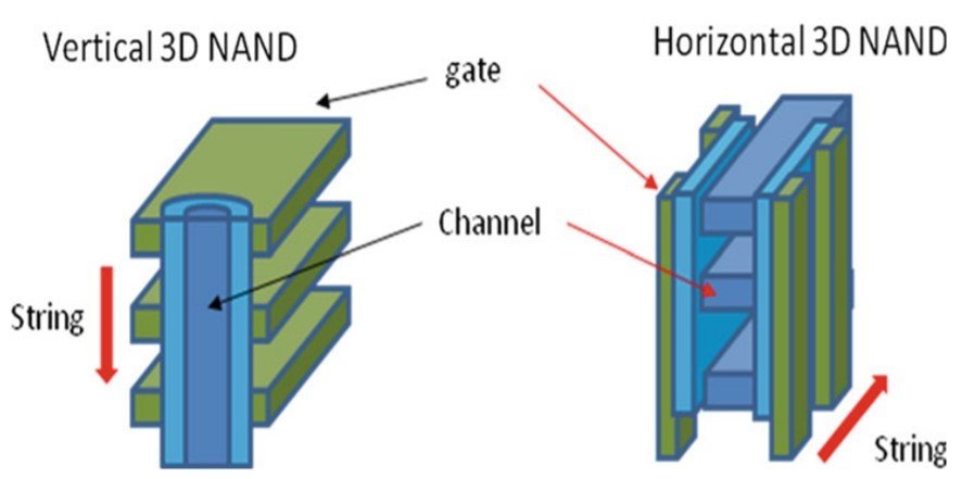
3D NAND architecture can be “vertical” or “horizontal,” as illustrated in Figure 4. In vertical 3D, the channel of NAND cells is made of dots that cross the layers of the gates, and the channel length of each transistor of the NAND string is determined by the thickness of the poly layer, while channel width is determined by the perimeter of the dot. To minimize the occupied area, the diameter of the dot is defined by the process-feature size. Gate layers are common to all cells of a bit-line and are not lithographically defined. In contrast, in the horizontal approach the gates rise vertically and are defined to build gate length, while channels run horizontally. In this case, channel width is defined by the thickness of the channel layer. The first 3D-based commercial NAND memory, released by Samsung in 2014, is based on a vertical 3D architecture.
FIgure 4. Vertical and horizontal 3D NAND.
As noted by Micheloni (2016), the promise of 3D NAND is that transition costs such as those with integration of new technology with SSD interfaces are “one time” costs that, once realized, will enable 3D NAND chips to achieve lower cost-per-bit values than those afforded by current planar NAND products. Micheloni (2016) anticipates that initial growth is likely to be concentrated in enterprise SSD solutions, as the client SSD segment has cooled somewhat in the second half of the 2010s. Lue (in Dimitrakis, 2015) notes that, were a 3D architecture to be implemented successfully, scaling of NAND Flash could be “reset,” meaning that designers could achieve ever greater bit densities while using feature sizes that were the norm in planar NAND years ago, only this time stacked and organized in a novel three-dimensional fashion. As a result, having at least one successful 3D NAND architecture could ensure scalability for the near future.
The time gap between the first publication on BiCS (an early 3D NAND architecture, described by Japanese researchers in 2007) and the commercial release of a 3D NAND product by Samsung (in 2014) was 7 years, an impressively small time-to-market for memory industry standards; such a short delay reflects the Flash community’s urgency in finding ways to surmount the limitations of existing NAND tech as scaling reaches the 20-nm node.
In addition to pursuing a different architecture, engineers have gone one step further and ditched the decades-old floating gate concept itself. In its place, designers have begun to employ charge-trapping (CT) memories, a technology that, in spite of its apparent novelty, was originally conceptualized in the 1960s. In a CT cell (Figure 5), carriers are injected and ejected through a tunnel oxide much like they would in a floating gate. However, in contrast to floating gate cells, which have a polycrystalline silicon layer as storage element, in a charge-trap memory electrons are trapped inside a silicon nitride film. A charge trap memory cell is obtained by intercalating a layer of Si3N4 between two insulating layers of SiO2, with a conductive layer of poly-Si as the control gate. The many electron traps contained in the nitride layer therefore play an equivalent role to that of a floating gate.
Figure 5. A charge-trap cell.
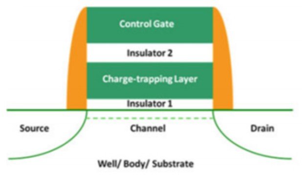
The tunnel oxide is typically 2 – 5 nm thick and allows electrons coming from the channel to move by tunneling into the thicker insulating SiN layer and to occupy the traps located inside the forbidden SiN band. Electrons are transferred by applying a positive voltage to the control gate.
One important advantage of charge-trap memory cells is that the control gate interacts directly with the electrons circulating in the channel. The shielding effect of the floating gate is no longer observed and, as a result, the issue of coupling between control gate and floating gate, a limiting factor in problems concerning miniaturization in FG cells, is no longer an issue.
Replacing the poly-Si-based conductive floating gate by an Si3N4 layer, which is insulating and rich in electron traps, also presents the advantage of storing the electrons in distinct areas of the insulator. As a result, achieving multiple-bit cells in charge trap designs is potentially easier than with floating gate technology (Lacaze and Lacroix, 2014).
8. Closing
Instead of making the copious investments associated with implementation with state-of-the-art NAND, engineers could simply get rid of Flash and come up with an entirely new storage technology. Novel non-volatile memory technologies such as ferroelectric RAMs (FeRAMs) have achieved reasonable success and discussions on them fill entire volumes (e.g., Park, 2016). Still, one advantage of NAND is that while emerging memories demand an entirely new process of integration with existing digital technologies, 3D NAND products, be they based on floating gate or charge trap cells, rely on over three decades of Flash research experience and can be readily integrated with present devices. Three-dimensional NAND designs have achieved reasonable degree of success and, combined with modern charge trap technology, may satisfy the bit density and affordable cost demands of the memory market for the near future.
References
For convenience, I listed edited books with the name of the editor because I used more than one chapter, and different chapters had different authors.
- Bez, R., Camerlenghi, E., Modelli, A. and Visconti, A. (2003). Introduction to Flash memory. Proceedings of the IEEE, 91:4, 489 – 502.
- BREWER, J.E. and GILL, M. (Eds.) (2008). Nonvolatile Memory Technologies with Emphasis on Flash. Hoboken: John Wiley and Sons.
- DIMITRAKIS, P. (Ed.) (2015). Charge-Trapping Non-Volatile Memories: Volume 1. Berlin/Heidelberg: Springer.
- GASTALDI, R. and CAMPARDO, G. (Eds.) (2017). In Search of the Next Memory. Berlin/Heidelberg: Springer.
- LACAZE, P.C. and LACROIX, J.-C. (2014). Non-Volatile Memories. Hoboken: John Wiley and Sons.
- MICHELONI, R. (Ed.) (2016). 3D Flash Memories. Berlin/Heidelberg: Springer.
- MICHELONI, R., MARELLI, A. and ESHGHI, K. (Eds.) (2018). Inside Solid State Drives (SSDs). 2nd edition. Berlin/Heidelberg: Springer.
- PARK, B.-E. et al. (Eds.) (2016). Ferroelectric-Gate Field Effect Transistor Memories. Berlin/Heidelberg: Springer.
- RICHTER, D. (2014). Flash Memories. Berlin/Heidelberg: Springer.
- SEIICHI, A. (2016). NAND Flash Memory Technologies. Hoboken: John Wiley and Sons.