
1. Intro to thermal oxidation of silicon
One of the major reasons for the popularity of silicon integrated circuits (ICs) is the ease with which silicon forms an excellent oxide, SiO2. Generally, SiO2 functions as an insulator in a number of device structures or as a barrier to diffusion or implantation during device fabrication. In the fabrication of a p–n junction, the SiO2 film is used to define the junction area.
High temperature is not strictly necessary to grow an oxide in a layer of pure silicon exposed to some oxygen-rich environment. However, at room temperature neither the silicon nor the oxygen molecules are appreciably mobile, and the oxidation reaction will not proceed beyond a thickness greater than 25 angstroms or so (Campbell, 2001). Subjecting the silicon-oxygen system to a high temperature, a process known as thermal oxidation, allows for thicker oxide layers and exponentially faster reactions.
Thermal oxidation of silicon is easily achieved by heating the wafer to a high temperature, typically 900 to 1200oC, in an atmosphere containing either pure oxygen or water vapor. Both water vapor and oxygen move (diffuse) easily through silicon dioxide at these high temperatures. The diffusivity of Si in SiO2 is several orders of magnitude smaller than the diffusivity of O2. As a result, the chemical reaction occurs at the Si-SiO2 interface. The chemical reaction occurring at the silicon surface is, for dry oxygen,

and, for water vapor,

Silicon is consumed as the oxide grows, and the resulting oxide expands during growth. The final oxide layer is approximately 54% above the original surface of the silicon and 46% below the original surface.
Water vapor has a much higher solubility than oxygen in silicon dioxide, which helps explain the much higher oxide growth rate in a wet atmosphere. However, the hydrogen molecules produced as a byproduct of wet oxidation may end up trapped in the silicon dioxide layer, which makes for a less dense oxide layer. Accordingly, dry oxidation may be preferred because it leads to denser, higher quality oxide, even though this may come at the cost of slower growth. Wet oxidation is used to grow thick layers such as masking, blanket field, and LOCOS oxides.
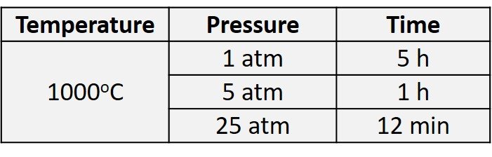
Increasing pressure increases the oxygen or steam concentration inside the processing chamber as well as the diffusion rate inside the silicon dioxide, which helps to increase the oxidation rate. High-pressure oxidation can reduce oxidation time at the same oxidation temperature, or reduce oxidation temperature at the same oxidation time. Generally, increasing pressure by one atmosphere can reduce oxidation time appreciably (Xiao, 2012). Table 1 shows time and temperature reductions caused by using a high-pressure oxidation process to grow a 10,000-angstrom (1-
Table 1. Oxidation time required to grow 10,000-angstrom wet oxide
Oxidation rate is also related to dopant concentrations. Heavily doped silicon generally oxidizes faster than lightly doped silicon. During oxidation, boron in the silicon tends to be drawn up into the silicon oxide, which causes depletion of the boron concentration at the Si-SiO2 interface. n-type dopants such as phosphorus, arsenic, and antimony have the opposite effect. When oxidation occurs, these dopants are driven deeper into the silicon. Similar to snow piling up from a snowplow, the n-type dopant concentration in the Si-SiO2 interface can become significantly higher than its original value. The results, in short, are a pile-up effect for n-type dopants and a depletion effect of p-type dopants.
Oxidation rate also depends slightly on silicon crystal orientation. Silicon of <111> orientation oxidizes faster than <100> silicon, with other orientations somewhere in between. The crystal orientation changes the number of silicon bonds available at the silicon surface, which influences the oxide growth rate and quality of the silicon-silicon dioxide interface (Jaeger, 2002).
2. More on the Si/SiO2 interface; use of chlorine gases
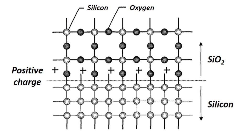
There is an abrupt transition at the oxide-silicon (Si/SiO2) interface between single crystal silicon to amorphous SiO2. Recall that for the SiO2 molecule, each silicon is bonded to four oxygen atoms and each oxygen atom is bonded to two silicon atoms. At the Si/SiO2 interface, some silicon atoms in the structure remain unbonded (see Figure 1). This incomplete oxidation of silicon less than 2 nm away from the Si/SiO2 interface is the origin of a positive fixed oxide charge. Other charges built up at the interface include an interface-trapped charge consisting of positive or negative charges that result from structural defects, oxidation-induced defects, or metal impurities, and a mobile oxide charge due to mobile ionic contaminants (MICs). There is also the possibility of an oxide-trapped charge that is positive or negative and trapped in the bulk of the oxide away from the interface. This accumulation of charge at the Si/SiO2 interface is undesirable for normal device operation and can cause the threshold voltage of a MOS device to shift to unacceptable values.
Figure 1. An illustration of charges and atoms at the Si-SiO2 interface.
Using a chlorine-containing gas during the oxidation process can serve to neutralize the charge accumulation at the interface (Quirk and Serda, 2001). In the presence of such a gas, chlorine ions diffuse to the positively charged layer and form a neutral layer. The chloride concentration is usually kept below 3% because excessive chloride ions may cause device instability. Another important advantage of addition of chloride ions to an oxidation process is the fact that they may enhance the oxide growth rate by up to 15%. What’s more, the presence of chlorine can actually immobilize (a process known as gettering) mobile ionic contaminants (MICs) that come from the furnace equipment, processing materials, and handling.
Early work used chlorine or vapor-phase hydrogen chloride (HCl). Chlorine is extremely toxic and HCl vapor in the presence of water vapor is corrosive. A common chlorine compound often used to transport the chlorine into the furnace is dichloroethylene (DCE) or variants of this compound. Other less-corrosive sources of chlorine are trichloroethylene (TCE) and 1,1,1-trichloroethane (TCA). TCE is carcinogenic and has fallen out of use, while TCA is a ozone-depleting chemical and has likewise disappeared from industrial practice. Some semiconductor manufacturers have switched back to HCl because of improvements in high-purity piping and fittings used to transport this chemical. In dry oxidation, HCl is used to remove mobile metallic ions, especially sodium, by forming immobile chloride compounds. This is very important, since a trace amount of Na can cause MOS transistor malfunction and affect IC chip performance and reliability.
3. The Deal-Grove model of thermal oxidation
One of the earliest and most widely used models of thermal oxidation of silicon is the Deal-Grove model. First published in the 1960s, it is a phenomenological macroscopic model that does not assume anything about the atomistic mechanisms of oxidation. Crucially, in the DG model oxygen diffusion process is assumed to be Fickian in nature, so it can be modeled by the simple diffusion equation
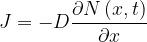
where J is the particle flux (particle flow per unit area), D is the diffusion coefficient, N is the particle concentration, x is the spatial coordinate in the direction of interest, and t is time. The system we employ to model thermal oxidation per the DG model is illustrated in Figure 2. In this system, we will make the approximation that the oxygen flux passing through the dioxide in Figure 2 is constant everywhere in the oxide. (Oxygen does not accumulate in the dioxide.)
Figure 2. Si-SiO2 interface in the Deal-Grove model.
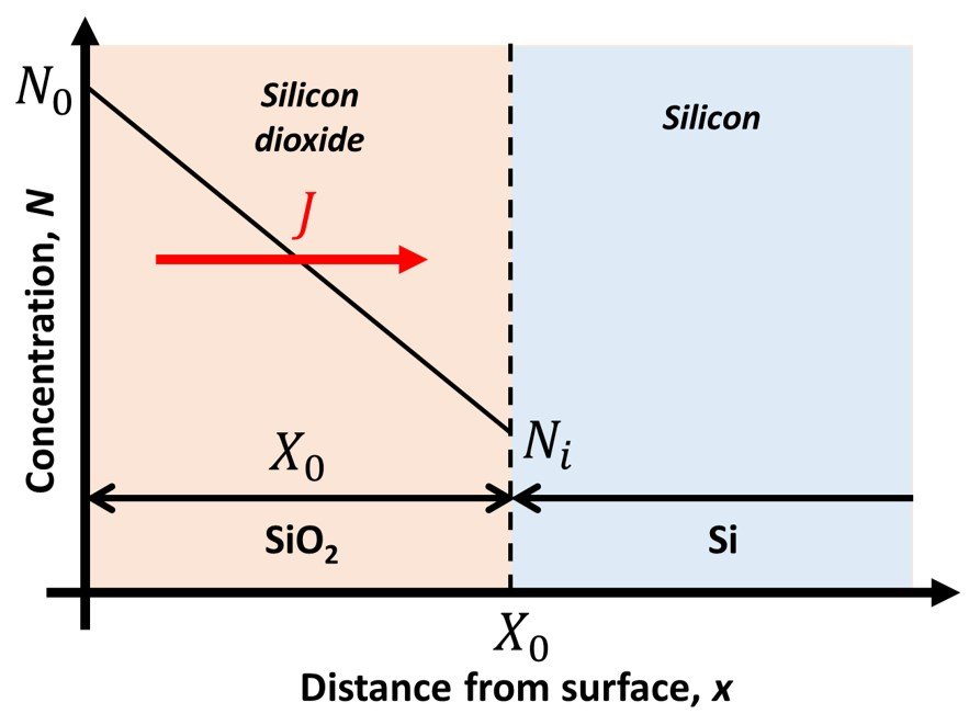
The oxygen flux J is then given by
where X0 is the thickness of the oxide at a given time, and N0 and Ni are the concentrations of the oxidizing species in the oxide at the oxide surface and silicon dioxide-silicon interface, respectively. At the silicon dioxide-silicon interface, we assume that the oxidation rate is proportional to the concentration of the oxidizing species so that the flux at the interface can be stated as

where ks is the rate constant for the reaction at the Si-SiO2 interface. Eliminating Ni using the two foregoing equations, the flux J can be restated as

The rate of change of thickness of the oxide layer with time is then given by the oxidizing flux divided by the number of molecules M of the oxidizing species that are incorporated into a unit volume of the resulting oxide:

This differential equation can be easily solved using the boundary condition that at t = 0 the thickness X0 of the oxide layer equals some fixed initial value Xi. The solution is
where
The parameters A and B are well known for a variety of process conditions, and are usually quoted in lieu of the more fundamental parameters that they incorporate, such as diffusivity and rate constant. Solving the expression above for X0(t) yields

This equation has two limiting forms. For sufficiently thin oxides one can neglect the quadratic terms and write

In this region, growth rate is limited by the reaction at the silicon interface. On the other hand, if the oxide is sufficiently thick the term that is linear in the thickness can be ignored and

In this region, oxidation rate is diffusion-limited. These two limiting situations are illustrated in Figure 3. Because of these two limiting forms, B/A is called the linear rate coefficient and B is called the parabolic rate coefficient. These are the numbers that are usually quoted for Deal-Grove thermal oxidation modelling.
Figure 3. Growth regimes in Deal-Grove thermal oxidation.

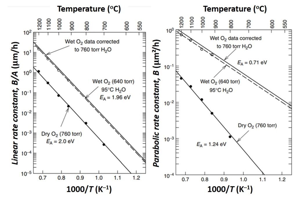
Experiments have indicated that both the linear rate coefficient B/A and the parabolic rate constant B increase exponentially with temperature, as indicated in Figure 4. The temperature dependence of B can be traced to that of the diffusion coefficient D, while the temperature dependence of B/A is primarily related to the kinetic reaction rate constant ks (Cleavelin et al., in Doering and Nishi, 2008). The pressure dependence of the rate constants has also been investigated, and results show that A is largely independent of pressure, while B is linearly dependent on pressure. Lastly, the crystal orientation dependence of the parabolic and linear rate constants indicate that the B/A for <111> silicon is an average of 1.68 times that of B/A for <100> silicon.
Figure 4. Variation of rate constants with temperature. EA denotes activation energy. From Cleavelin et al. (2008).
It is worth pointing out the significance of 
The Deal-Grove model for oxidation has provided good agreement over the given range of experimental conditions, with the exception of dry oxidation films with thicknesses less than approximately 30 nm. For thicknesses less than 30 nm the oxidation rate was predicted to be faster than that predicted by the DG model. Several phenomena have been tentatively proposed to explain the growth rate enhancement at exceptionally thin oxide thicknesses, including field-enhanced oxidation, structural effects such as microchannels, stress effects modifying the oxidant diffusivity, and changes in the oxygen solubility in the oxide (Cleavelin et al., in Doering and Nishi, 2008).
4. Oxide thickness and the color chart
Monitoring the oxidation process means measuring oxide thickness and its uniformity. Techniques used in oxide thickness determination may be electrical, optical, and physical in nature and include ellipsometry, profillometry, transmission electron microscopy (TEM), X-ray photoelectron spectroscopy (XPS), medium energy ion scattering spectrometry (MEIS), nuclear reaction analysis (NRA), Rutherford backscattering (RBS), and elastic backscattering spectrometry (EBS). Ellipsometry is one of the oldest and cheapest techniques. It is based on the polarization changes that occur when light is reflected from or transmitted through a medium. Changes in polarization are functions of the optical properties of the material (i.e., its complex refractive indices), its thickness, and the wavelength and angle of incidence of the light beam relative to the surface normal. These differences in polarization are measured by an ellipsometer, and the oxide thickness can then be calculated.
After the oxide is grown, the color of the wafer surface changes. Color depends on film thickness, refractive index, and the angle of light. Reflected light from the oxide surface (light 1 in Figure 5) and reflected light from the Si-SiO2 interface (light 2) have the same frequencies, but with different phases, light 2 travels a longer distance inside the oxide film, as shown in Figure 5. The two reflected lights interfere with each other and cause both constructive and destructive interference at different wavelengths, since the refractive index is a function of wavelength. Constructive interference leads to enhancement of a certain wavelength of reflected light, and the color of the wafer corresponds to that wavelength. For example, a wafer with a 390-nm thick silicon dioxide layer will appear yellow (Table 2).
Figure 5. Reflected light and phase difference.
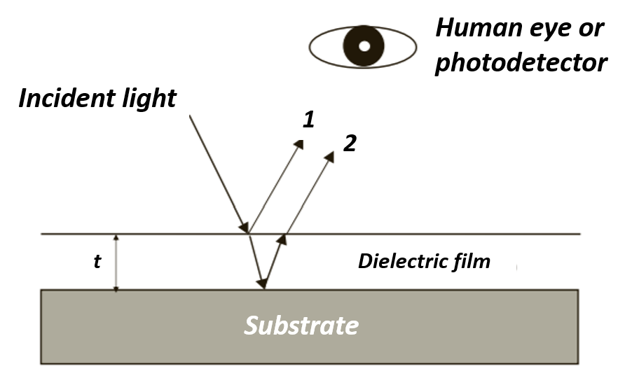
Table 2. Silicon oxide thickness-color chart.
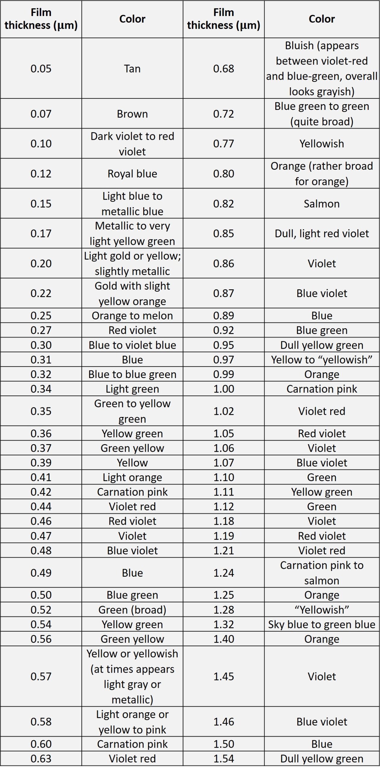
It goes without saying that color chart comparisons are subjective in nature and offer only an educated guess of oxide thickness. For more accurate estimates, recourse must be made to one of the advanced techniques mentioned above.
References
• CAMPBELL, S.A. (2001). The Science and Engineering of Microelectronic Fabrication. 2nd edition. Oxford: Oxford University Press.
• Cleavelin, C.R., Colombo, L., Niimi, H. et al. (2008). Oxidation and gate dielectrics. In: DOERING, R. and NISHI, Y. (Eds.). Semiconductor Manufacturing Technology. 2nd edition. Boca Raton: CRC Press.
• JAEGER, R.C. (2002). Introduction to Microelectronic Fabrication. 2nd edition. Upper Saddle River: Prentice Hall.
• MAY, G.S. and SZE, S.M. (2003). Fundamentals of Semiconductor Fabrication. Hoboken: John Wiley and Sons.
• QUIRK, M. and SERDA, J. (2001). Semiconductor Manufacturing Technology. Upper Saddle River: Prentice Hall.
• XIAO, H. (2012). Introduction to Semiconductor Manufacturing Technology. 2nd edition. Bellingham: SPIE Press.